Reporter: Zenaida Alzaga / Photographer: Jorge Aguilar
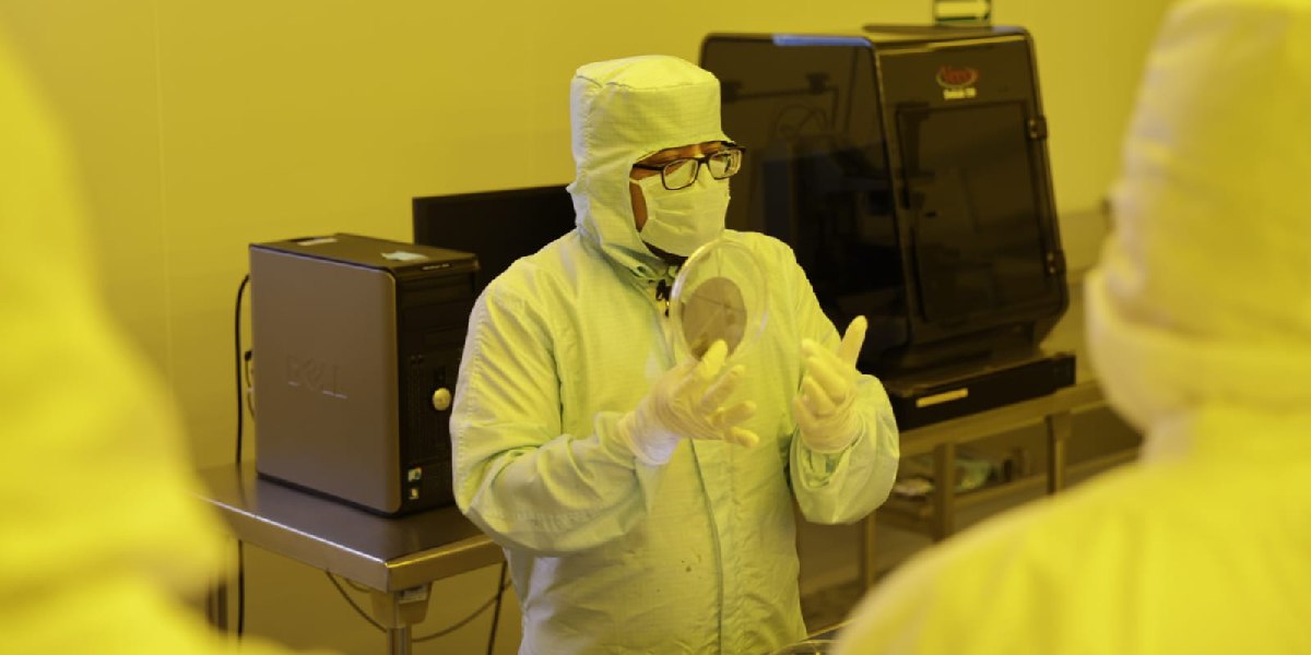
Semiconductors are tested to ensure their performance under extreme conditions.
The Instituto Politécnico Nacional (IPN), through its Center for Nanosciences and Micro and Nanotechnologies (CNMN), is engaged in Assembly, Testing, and Packaging (ATP) processes for the production of semiconductors and integrated circuits—key components for a wide range of industrial applications.
During his participation in the roundtable “Assembly, Testing, and Packaging in Mexico,” held as part of the Summer School on Semiconductor Devices and Integrated Circuits 2025, Dr. Salvador Mendoza Acevedo, CNMN researcher, explained that during the ATP phase, these devices undergo various laboratory tests to prepare and evaluate their performance under extreme temperatures, radiation, humidity, and other challenging conditions.
These procedures, he noted, help ensure proper functionality while enabling the development of smaller, more complex, and more advanced devices to meet the evolving demands of the productive sector and support scientific and technological progress.
In the panel of experts, Jesús Javier Alcantar Peña, from the Center for Engineering and Industrial Development (CIDESI), and Carlos Meneses, from the U.S.-Mexico Foundation for Science (FUMEC), stated that the semiconductor sector requires stronger cybersecurity protocols in the design, manufacturing, and infrastructure phases, as these systems are vulnerable to hacking.
They also stressed the need to streamline the processes for registering patents and intellectual property related to these technologies.
Mexico, they added, has a highly skilled workforce in electronics, quality control, production, assembly, and chip packaging. However, to fully tap into the North American market, the country must offer greater tax incentives and implement simpler mechanisms to encourage companies to establish or expand operations within the national territory.
As part of the academic activities, students participated in a Photolithography Workshop, where they worked on the design and fabrication of semiconductors; in the Organic TFT Modeling module; and a course on Analog Integrated Circuit Design using open-source tools.

INSTITUTO POLITÉCNICO NACIONAL
D.R. Instituto Politécnico Nacional (IPN). Av. Luis Enrique Erro S/N, Unidad Profesional Adolfo López Mateos, Zacatenco, Alcaldía Gustavo A. Madero, C.P. 07738, Ciudad de México. Conmutador: 55 57 29 60 00 / 55 57 29 63 00.
Esta página es una obra intelectual protegida por la Ley Federal del Derecho de Autor, puede ser reproducida con fines no lucrativos, siempre y cuando no se mutile, se cite la fuente completa y su dirección electrónica; su uso para otros fines, requiere autorización previa y por escrito de la Dirección General del Instituto.
