• At the National Laboratory of Micro and Nanotechnologies (LNunT), highly skilled professionals are trained to develop these technological devices.
• The facility also prepares top-tier specialists for the design, development, and production of semiconductors required by the national and international industry
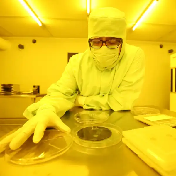
In response to the growing global demand for electronic microdevices, the Instituto Politécnico Nacional (IPN), through the National Laboratory of Micro and Nanotechnologies (LNunT), operates a Class 100 (ISO 5) cleanroom, where scientists work on the design and fabrication of semiconductors, as well as on processes linked to the supply chain, in full compliance with industry standards and the needs of the IPN community.
This was highlighted by researchers Jacobo Esteban Munguía Cervantes and Francisco Javier Hernández Cuevas, who explained that the Laboratory trains highly qualified professionals in semiconductor production to support national industry, while also advancing research in microelectronics, nanotechnology, microelectromechanical systems (MEMS) assemblies, solar cells, thin-film devices, sensors, and other areas that require particle-free environments.
The work carried out at these facilities aligns with the policy guidelines established by President Claudia Sheinbaum Pardo and the Secretary of Public Education, Mario Delgado Carrillo.
The defining feature of a cleanroom lies in its purity levels. The IPN facility is equipped with ULPA (Ultra-Low Particulate Air) filters, capable of retaining particles as small as 0.1 micrometers, and provides laminar airflow across an area of 200 square meters. This configuration ensures a controlled environment that remains within the limits established by applicable regulations.
Cleanrooms are essential for semiconductor design and development, as purity levels are critical: excessive particle presence can impair device performance, particularly when components are manufactured at the nanometric scale—equivalent to one-millionth of a millimeter.
The National Laboratory is part of the Institute’s Center for Nanosciences and Micro and Nanotechnologies (CNMN) and holds certification from the Ministry of Science, Humanities, Technology, and Innovation (Secihti, formerly Conahcyt).
At the global level, the researchers noted, there is a strong demand for professionals specialized in semiconductor manufacturing. In this context, the IPN has the tools, cleanroom infrastructure, and trained personnel required to educate engineers in this strategic field.
In semiconductor production, scientists primarily use silicon (Si), a material essential for manufacturing electronic devices such as microprocessors, cell phones, chips, and nano- and micro-scale processors.
Munguía Cervantes and Hernández Cuevas added that, beyond working on device development and supply chains, the Laboratory also supports various academic units within the Institute, including the Higher School of Medicine (ESM), by producing micrometer-scale semiconductors for the early diagnosis of diseases such as cancer.
Finally, they emphasized that LNunT’s certification enables the application of advanced techniques for processor fabrication, design, and characterization at different scales, as well as the integration of layers tailored to industry needs and data-transfer requirements—resulting in faster, more responsive devices.
For more information, visit www.ipn.mx

INSTITUTO POLITÉCNICO NACIONAL
D.R. Instituto Politécnico Nacional (IPN). Av. Luis Enrique Erro S/N, Unidad Profesional Adolfo López Mateos, Zacatenco, Alcaldía Gustavo A. Madero, C.P. 07738, Ciudad de México. Conmutador: 55 57 29 60 00 / 55 57 29 63 00.
Esta página es una obra intelectual protegida por la Ley Federal del Derecho de Autor, puede ser reproducida con fines no lucrativos, siempre y cuando no se mutile, se cite la fuente completa y su dirección electrónica; su uso para otros fines, requiere autorización previa y por escrito de la Dirección General del Instituto.